Are you trying to understand how MOSFETs are structured and how they work?
Do you want to learn the working principle of both N-channel and P-channel MOSFETs?
If so, you’re in the right place.
I’ve been working as an electronic circuit design engineer for about 10 years.
When I was a beginner, I clearly understood the structure of bipolar transistors,
but I couldn’t quite grasp how MOSFETs were built or how they actually operated.
Now that I’ve mastered these concepts through practical design experience,
I’ll explain them in a clear and simple way.
By the end of this article, you’ll understand the structure and working principle of MOSFETs —
both N-channel and P-channel types.
It only takes about 3 minutes to read, so let’s get started!
Structure and Working Principle of MOSFETs
The structure of MOSFETs can be broadly classified into four types:
- N-channel MOSFET (Enhancement type)
- N-channel MOSFET (Depletion type)
- P-channel MOSFET (Enhancement type)
- P-channel MOSFET (Depletion type)
They can be categorized in two ways:
First, depending on the type of charge carriers that flow through the MOSFET — whether they are negative or positive.
Negative charge carriers → N-channel MOSFET
Positive charge carriers → P-channel MOSFET
Second, based on the conduction state of the MOSFET when the input signal to the gate terminal is zero — whether the device is normally OFF or normally ON.
When the MOSFET is OFF at zero gate voltage → Enhancement type
When the MOSFET is ON at zero gate voltage → Depletion type
Let’s look at each type in detail.
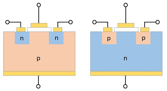
Structure of N-Channel MOSFETs
Enhancement-Type and Depletion-Type N-Channel MOSFETs
【N-channel MOSFET (Enhancement type)】
When the gate voltage is zero, no channel is formed between the source and drain.
【N-channel MOSFET (Depletion type)】
When the gate voltage is zero, a conductive channel already exists between the source and drain.
The structural diagrams of N-channel MOSFETs are shown above.
As mentioned earlier, when the input signal to the gate terminal is zero, the MOSFET’s conduction state determines whether it is an enhancement-type or depletion-type device.
In other words, as you can see from the figures above, it depends on whether a channel is formed or not when the gate voltage is zero.
In the case of an enhancement-type MOSFET, the channel is not formed.
In contrast, for a depletion-type MOSFET, the channel is already formed.
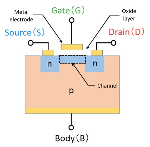
The channel is essentially the path through which current flows.
Current flows from the drain to the source through this channel.
In other words,
When the channel is not formed, the drain–source path is non-conductive.
When the channel is formed, the drain–source path becomes conductive.
That’s the basic structural difference between enhancement and depletion types.
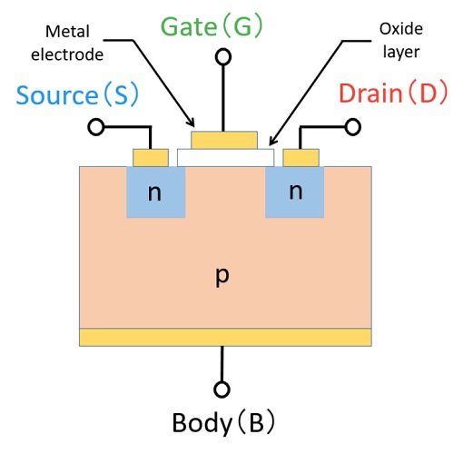
Does a MOSFET Have Four Terminals?
As shown in the structural diagrams, a MOSFET has four terminals: Gate (G), Drain (D), Source (S), and Body (B).
Wait — isn’t a MOSFET supposed to have only three terminals: Gate, Drain, and Source?
What is the Body (B) terminal?
That’s a common question. Indeed, in circuit diagrams and datasheets, MOSFETs are usually shown as three-terminal devices.
However, inside the MOSFET package, the Body (B) is internally connected to the Source (S).
Therefore, when used as an electronic component, a MOSFET is treated as a three-terminal device.
The Body terminal is also referred to as the bulk or back gate.
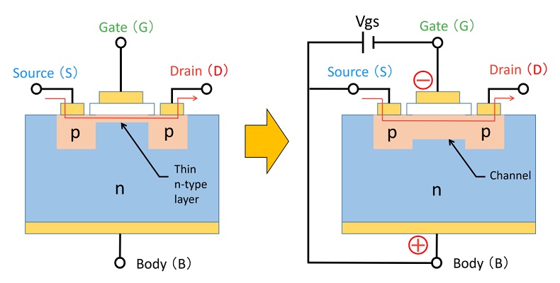
Operating Principle of N-Channel MOSFETs
Operation of the Enhancement-Type MOSFET
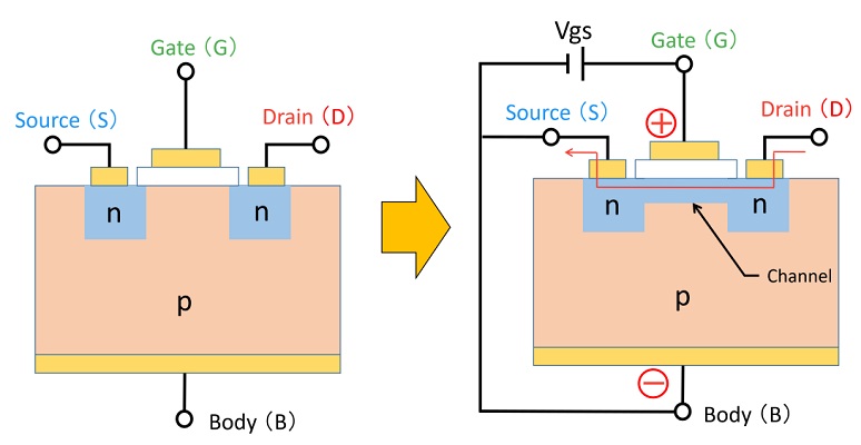
A channel is formed when a positive gate voltage is applied.
In the N-type semiconductor region (the blue area in the figure), there are many negative charge carriers and a small number of positive ones.
Conversely, in the P-type semiconductor region (the orange area), there are many positive charge carriers and only a few negative ones.
When a voltage VGS is applied between the gate and source terminals,
the gate terminal becomes positive, and the body terminal becomes negative.
(The source and body terminals are internally connected inside the MOSFET package.)
As a result, positive charge carriers in the P-type semiconductor move toward the body terminal,
and negative charge carriers move toward the gate terminal.
In other words, positive charges are repelled away from the gate region,
and negative charges accumulate near the gate terminal.
This accumulation of negative charges forms a channel.
Once the channel is formed, current can flow between the drain and source terminals.
As the applied gate–source voltage VGS increases, the channel becomes thicker, allowing more current to flow through the MOSFET.
Operation of the Depletion-Type MOSFET
The key difference from the enhancement-type is that when VGS = 0, a thin N-type layer (channel) already exists.
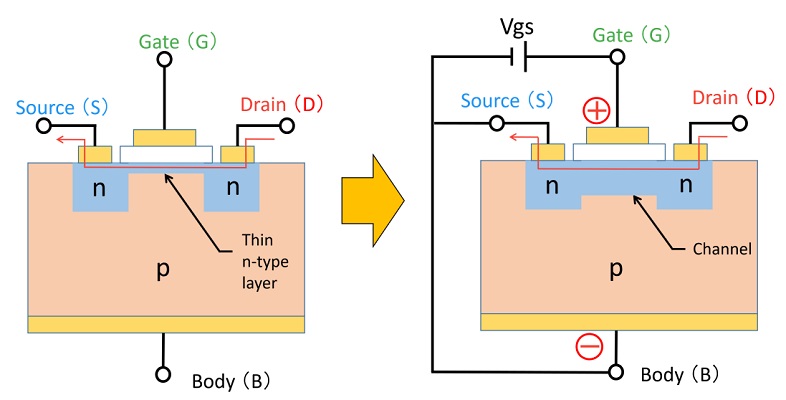
A channel already exists even when VGS = 0.
This means that current can flow between the drain and source terminals even when the gate–source voltage is zero.
Similar to the enhancement-type MOSFET, increasing the applied VGS enlarges the channel and allows more current to flow.
On the other hand, when a negative gate voltage is applied (the gate becomes negative and the body becomes positive),
the channel becomes thinner, and it becomes more difficult for current to flow between the drain and source.
Structure of P-Channel MOSFETs
Enhancement-Type and Depletion-Type P-Channel MOSFETs
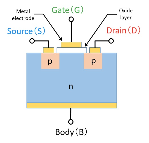
【P-channel MOSFET (Enhancement type)】
【P-channel MOSFET (Depletion type)】
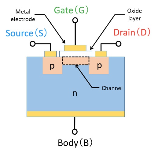
The structural diagrams of P-channel MOSFETs are shown above.
Compared with the N-channel MOSFET structure, the positions of the N-type and P-type semiconductor regions are simply reversed.
Just like in the N-channel MOSFET, the P-channel type can also be classified as either enhancement or depletion type, depending on whether a channel is formed when the gate voltage is zero.
In an enhancement-type MOSFET, the channel is not formed when the gate voltage is zero,
while in a depletion-type MOSFET, the channel already exists under the same condition.
In other words, the structure is fundamentally the same as that of an N-channel MOSFET, only with opposite semiconductor types.
Operating Principle of P-Channel MOSFETs
Operation of the Enhancement-Type MOSFET
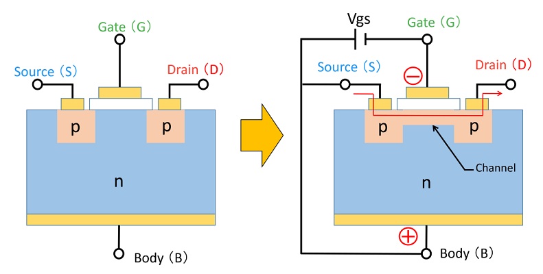
The polarity of voltages and charge carriers is opposite to that of the N-channel type.
As explained in the operation of the N-channel MOSFET, the N-type semiconductor contains many negative charge carriers and only a few positive ones.
Conversely, the P-type semiconductor contains many positive charge carriers and only a few negative ones.
When a negative gate–source voltage (−VGS) is applied,
the gate terminal becomes negative, and the body terminal becomes positive.
(The source and body terminals are internally connected inside the MOSFET package.)
As a result, negative charge carriers are repelled away from the gate region,
and positive charge carriers gather near the gate terminal.
This accumulation of positive charge forms a channel, allowing current to flow between the drain and source terminals.
As the magnitude of the negative gate–source voltage (−VGS) increases, the channel becomes thicker and can conduct a larger current.
In short, compared with the operation of an N-channel MOSFET, the polarities of voltage and charge carriers are simply reversed.
Operation of the Depletion-Type MOSFET
The key difference from the enhancement-type MOSFET is that when VGS = 0, a thin p-type layer is already formed beneath the gate region.
A thin p-type layer is already formed when VGS = 0, allowing current to flow between the drain and source.
Because of this, current can flow between the drain and source even when the gate–source voltage is zero.
Just like in the enhancement-type MOSFET, increasing the magnitude of the negative gate–source voltage (−VGS) makes the channel thicker and allows more current to flow.
In short, the behavior of the depletion-type P-channel MOSFET is essentially the same as that of the N-channel version.
Let’s Build a Circuit and See How It Works!
If you want to understand MOSFET operation more deeply, try building and testing a simple circuit yourself!
Example Circuit
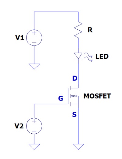
It’s easiest to experiment with an N-channel enhancement-type MOSFET.
You can clearly see how the LED turns ON or OFF depending on whether a gate–source voltage (VGS) is applied.
When VGS is applied:
→ A channel is formed
→ Current flows from the drain (D) to the source (S)
→ The LED lights up
When VGS = 0V:
→ The channel is not formed
→ No current flows from the drain (D) to the source (S)
→ The LED stays OFF
In this way, you can visually confirm the MOSFET’s operating principle by observing whether the LED turns on or off.
Components You’ll Need
In this experiment, you can easily understand how a MOSFET operates by observing whether the LED turns ON or OFF.
- N-channel MOSFET: 2N7000
-
An enhancement-type N-channel MOSFET ideal for LED lighting and switching experiments.
It’s one of the most widely used beginner-friendly MOSFETs and easy to handle for first-time users. - Resistor Set
-
Use resistors between 330 Ω and 1 kΩ for LED circuits.
For basic experiments, 1/4 W resistors are sufficient, but use 1/2 W or higher when handling larger currents. - LED Set
-
LEDs emit light when current flows through them.
Having multiple colors—red, yellow, green, blue, and white—makes experiments more engaging and easier to observe. - Breadboard (830 holes)
-
A solderless breadboard allows you to build and modify circuits easily by inserting components.
Perfect for beginners and quick prototyping. - Jumper Wire Set
-
Used to connect components on the breadboard.
Having male–male, male–female, and female–female jumper wires provides the best flexibility for different setups. - USB 5 V Breadboard Power Module
-
Provides a stable 5 V or 3.3 V supply directly to the breadboard.
Very convenient for powering low-voltage circuits safely. - Digital Multimeter (Tester)
-
Use a digital multimeter to measure voltage and current and confirm how the MOSFET is switching.
Start with an affordable, simple model—perfect for basic electronics learning.
Important Notes
MOSFET pin configurations may vary depending on the manufacturer and model.
Also, the maximum voltage and current ratings differ by product.
Always check the datasheet for pin layout and ratings before building your circuit.
Useful Tools for Measurement
When experimenting, you might wonder: “Is current really flowing?” or “Is the MOSFET switching properly?”
- To easily check voltage and current: → Digital Multimeter
- To observe signal waveforms: → Oscilloscope
- To power your circuit safely with a stable source: → DC Power Supply
Check out these tools if you’d like to measure or observe the actual behavior of your circuit.
Summary
In this article, we explained the structure and operating principle of MOSFETs.
MOSFETs are widely used in electronic circuits for switching, motor control, and many other applications.
By understanding how MOSFETs work,
you’ll be able to apply this knowledge to your own electronic projects and circuit designs.
Related Articles
Bonus: MOSFET Materials
MOSFET technology continues to improve every year, offering better performance and higher efficiency.
The MOSFETs introduced in this article are the most common type, made from silicon (Si), which is widely used in semiconductor devices.
In recent years, silicon carbide (SiC) has been used as a material to create high-performance MOSFETs with low ON-resistance and high breakdown voltage.
Power MOSFETs also achieve high performance—such as low ON-resistance and low power loss—through advanced structures like DMOS (Double-Diffused MOSFET) and SJ (Super Junction) designs.
That said, you don’t need to fully understand terms like SiC, DMOS, or SJ structure to start using MOSFETs. The concepts of structure and operation covered in this article are more than enough for practical understanding.
If this article helped you think, “So that’s how a MOSFET works!”, then that’s exactly the goal. For the finer details, you can always refer to the electrical characteristics listed in the MOSFET’s datasheet.
I hope this article helps you better understand how MOSFETs work and inspires you to experiment with them in your own circuits.