- Want to understand the structure of a bipolar transistor?
- Curious about how a transistor actually works?
- Not sure what current amplification really means?
This article will answer those questions.
I’ve been studying and designing electronic circuits for about 10 years.
The structure and working principle of transistors are among the most fundamental topics in electronics.
But interestingly, the more experience you gain, the easier it is to forget the basics.
This guide is written for both beginners who are just getting started with electronic circuits,
and experienced readers who might be wondering, “How does a transistor really work again?”
Let’s clearly explain the structure, operation, and amplification principle of transistors in an easy-to-understand way.
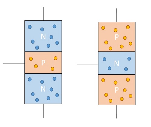
Structure of a Bipolar Transistor
There are two types of transistor structures.
One is the NPN transistor, where a thin layer of p-type semiconductor is sandwiched between two n-type semiconductors,
and the other is the PNP transistor, where a thin layer of n-type semiconductor is sandwiched between two p-type semiconductors.
NPN Transistor Structure
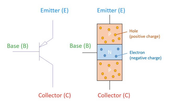
the base layer (P-type) is sandwiched between two N-type layers.
Electrons (negative charge) and holes (positive charge) are shown.
PNP Transistor Structure
the base layer (N-type) is sandwiched between two P-type layers.
The direction of electron and hole movement is opposite to that of the NPN transistor.
Each terminal is called the Emitter (E), Base (B), and Collector (C).
To make a transistor operate, a power supply must be connected to these terminals,
and a specific voltage must be applied between certain semiconductor layers.
Note that the transistor discussed here refers to a bipolar junction transistor (BJT).
Working Principle of a Transistor
Working Principle of a PN Junction Diode
The operation of a transistor is based on the working principle of a PN junction diode.
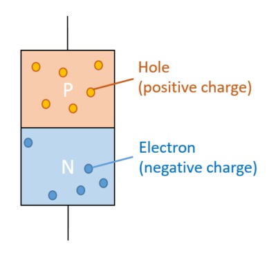
the p-type region contains holes (positive charge)
and the n-type region contains electrons (negative charge).
A PN junction diode has a rectifying property — it allows current to flow only in one direction.
When an external voltage is applied so that the p-type semiconductor is at a higher potential than the n-type semiconductor, current flows through the junction.
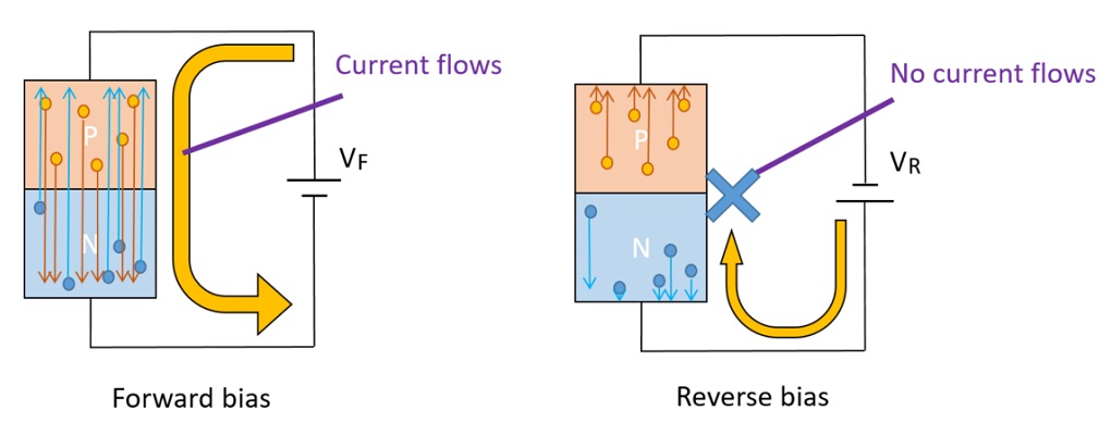
current flows under forward bias (VF)
but does not flow under reverse bias (VR).
At the junction between the p-type and n-type semiconductors, there exists a region called the depletion layer.
When a forward bias is applied, this depletion layer becomes narrower, allowing electrons (negative charge) and holes (positive charge) to move across the junction, resulting in current flow.
When a reverse bias is applied, the depletion layer widens, preventing charge carriers from crossing the junction — thus, no current flows.
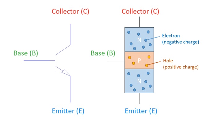
Working Principle of an NPN Transistor
A transistor operates by applying external voltages as shown in the figure below.
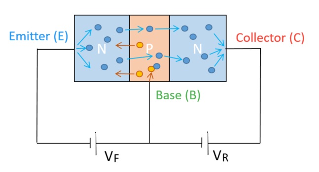
electrons move from the emitter to the collector
when a forward bias (VF) and reverse bias (VR) are applied.
When a forward voltage VF is applied between the base and emitter,
electrons from the emitter region (n-type) move into the base region (p-type).
In the base region, these electrons that enter the p-type layer move toward the collector region (n-type).
During this movement, some electrons recombine with holes and disappear.
You might wonder: why do electrons in the p-type base move toward the collector side?
That’s because the middle p-type layer is made very thin.
When a forward voltage is applied between the base and emitter, electrons from the emitter travel toward the p-type base.
Since this p-type region is thin, most electrons pass through it and continue into the collector (n-type) region.
There is another reason for making the base thin.
By narrowing the base layer, most electrons that enter from the emitter do not recombine with holes in the base, allowing them to reach the collector more efficiently.
Once electrons reach the collector region, they are attracted to the collector terminal by the reverse voltage (VR) applied across the collector-base junction.
Thus, electrons emitted from the emitter reach the collector terminal through the base region.
The direction of current flow is opposite to the direction of electron flow,
so current flows from the Collector (C) to the Emitter (E).
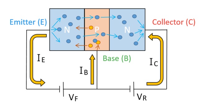
the emitter current (IE) splits into base current (IB) and collector current (IC)
when forward and reverse biases are applied.
The emitter current (IE) depends on the magnitude of the forward voltage (VF) applied between the base and emitter.
The higher the forward voltage, the greater the number of electrons that move through the junction.
The collector current (IC) is almost equal to the emitter current (IE).
This is because the p-type base is very thin, and recombination between electrons and holes rarely occurs.
In other words, to change the collector current, you only need to adjust the emitter current.
Working Principle of a PNP Transistor
When analyzing a PNP transistor, simply reverse the roles of electrons and holes and reverse the direction of the applied voltages (VF and VR).
As a result, the emitter–base junction is forward-biased just as in the NPN transistor,
and the base–collector junction is reverse-biased.
This allows holes (positive charge) from the emitter to move toward the collector,
causing the emitter and collector currents to flow in the opposite direction compared to an NPN transistor.
Principle of Current Amplification
A transistor has a characteristic that allows a small input current to produce a much larger output current.
This is called the current amplification effect. There are two major types of transistor amplifier circuits:
- Common-base connection — the type explained so far
- Common-emitter connection
Current Gain in the Common-Base Connection
In a common-base connection, as explained earlier, a forward voltage is applied between the base and emitter, and a reverse voltage is applied between the base and collector.
The current gain of this circuit is expressed by the parameter hFB (current gain in common-base configuration):
hFB = IC / IE
The typical value is around hFB = 0.995, which means hFB ≒ 1.
In other words, IE ≒ IC. The emitter current and collector current are almost the same.
This is because the middle p-type semiconductor layer of the NPN transistor is made very thin, so that most of the electrons from the emitter pass through without recombining with holes in the base region.
Therefore, although a transistor is said to amplify current, in a common-base configuration the current gain hFB is almost 1.
If you are wondering, “Then where does the amplification happen?”, the answer lies in the common-emitter connection described next.
Current Gain in the Common-Emitter Connection
The common-emitter amplifier circuit is shown below.
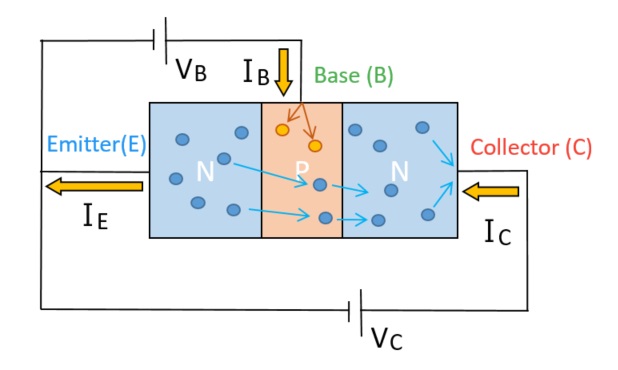
a small base current (IB) controls a much larger collector current (IC).
The current gain in a common-emitter configuration is expressed by hFE:
hFE = IC / IB
This can also be expressed in terms of hFB as follows:
hFE = IC / IB
= IC / ( IE − IC )
= ( IC / IE ) / ( 1 − ( IC / IE ) )
= hFB / ( 1 − hFB )
If hFB = 0.995, then:
hFE = 0.995 / ( 1 − 0.995 ) = 199 ≒ 200
Therefore, the current gain hFE in a common-emitter configuration can reach about 200 times.
In other words, a small base current IB can control a much larger collector current IC.
Because of this strong amplification property, the common-emitter configuration is widely used in electronic circuits.
Try It Yourself!
Once you understand the structure and working principle of a transistor, try building an actual circuit.
By observing how the LED lights up, you can visualize how current flows through the transistor.
Example Circuit
This is a basic NPN transistor circuit to observe current amplification.
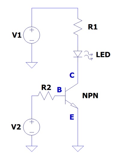
When a small current flows into the base terminal (B),
a much larger current flows from the collector (C) to the emitter (E), lighting up the LED.
This is called the current amplification effect.
Apply voltage to the base terminal (B) through a resistor
→ A small base current flows
→ Current flows between collector and emitter
→ The LED lights up
No voltage applied to the base terminal (0 V)
→ No current flows into the base
→ No current flows between collector and emitter
→ The LED remains off
Through this experiment, you can experience how a transistor controls current with current.
Components You’ll Need
Here are the components required to build a transistor current amplification circuit using a breadboard.
- NPN Transistor: 2N3904
-
A basic small-signal transistor ideal for beginner experiments.
By applying a small base current, you can light up an LED and observe the principle of current amplification. - Resistor Set
-
Use resistors between 330 Ω and 10 kΩ to test transistor operation.
1/4 W is usually sufficient, but use 1/2 W or higher for higher current circuits. - LED Set
-
LEDs emit light when current flows through them.
Prepare several colors (red, yellow, green, etc.) to compare brightness at different current levels. - Breadboard (830 holes)
-
A solderless breadboard that allows easy circuit assembly by inserting components.
You can easily change resistors to observe different behaviors. - Jumper Wire Set
-
Wires used to connect components on the breadboard.
Having male–male, male–female, and female–female wires provides flexibility for experiments. - USB 5V Breadboard Power Module
-
Supplies 5 V or 3.3 V power directly to the breadboard.
Perfect for powering LEDs or transistor test circuits. - Digital Multimeter (Tester)
-
Measure the voltage and current between the base, collector, and emitter.
This helps confirm the transistor’s current amplification behavior.
Important Notes
Transistor pin layouts vary depending on the model and manufacturer.
Also, the maximum voltage and current ratings differ by product.
Always check the datasheet before connecting components to ensure correct pin assignment and safe operation.
Useful Measurement Tools
By measuring voltage and current, you can gain a deeper understanding of transistor operation.
- To easily check voltage and current: → Digital Multimeter
- To observe signal waveforms: → Oscilloscope
- To power your circuit safely with a stable source: → DC Power Supply
Conclusion
In this article, we explained the structure and working principle of a transistor.
Was it helpful for you to understand how transistors actually work inside?
Even if you already have experience designing electronic circuits,
you might not often think about what’s really happening inside the transistor.
Over time, it’s easy to forget these fundamental concepts,
I hope this article helps you refresh your understanding of transistor operation and inspires you to explore electronics more deeply.
Related Articles
Bonus: Relationship Between Transistor Structure and ICs
The transistor structure you learned in this article is also used inside integrated circuits (ICs) — in fact, ICs contain countless transistors.
For example, logic circuits such as AND, OR, and NOT gates or operational amplifiers (op-amps)
are fundamentally made by combining multiple transistors together.
While a single transistor functions as a switch or an amplifier,
combining many of them enables signal processing, computation, and memory operations.
Understand each transistor individually
→ Combine them to form circuits
→ Combine countless circuits to create ICs (Integrated Circuits)
Keeping this connection in mind will help you deepen your understanding of how electronic circuits work as a whole.