- I want to understand the static characteristics of a MOSFET.
- I want to learn the input characteristics (VGS–ID) and output characteristics (VDS–ID).
- What are the saturation region and the pinch-off voltage?
This article will answer these common questions.
I have been working as an electronic circuit designer for about 10 years.
When designing MOSFET-based circuits, I always refer to the characteristic curves in the datasheet to select the optimal device.
Based on that experience, I will explain everything clearly and practically.
By the end of this article, you will be able to understand MOSFET characteristics while reading a datasheet with confidence.
It only takes a few minutes to read — I hope you find it helpful.
What Are MOSFET Static Characteristics?
Static characteristics of a MOSFET refer to the following two behaviors.
- Input characteristics (VGS–ID curve)
- Output characteristics (VDS–ID curve)
VGS: Gate–Source voltage
VDS: Drain–Source voltage
ID: Drain current
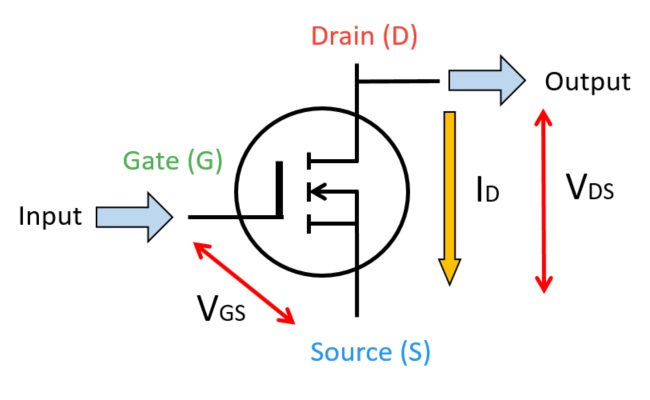
The input characteristics show how the drain current ID changes when VGS is varied.
The output characteristics show how the drain current ID changes when VDS is varied.
In the following sections, we will look at these characteristics using the actual graphs from a MOSFET datasheet.
Understanding Input and Output Characteristics Using a MOSFET Datasheet
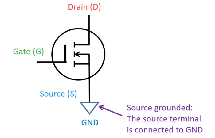
The characteristic curves shown in a MOSFET datasheet represent its static characteristics with the source terminal grounded.
This is because in real electronic circuits, the MOSFET is most commonly used with the source terminal connected to ground.
*Source-grounded means a circuit where the MOSFET’s source terminal is connected directly to GND.
As an example, let’s look at the Toshiba N-channel MOSFET 2SK2232.
We will examine both the “input characteristics (VGS–ID)” and “output characteristics (VDS–ID).”
Input Characteristics (VGS–ID Curve)
The input characteristic curve is shown below.
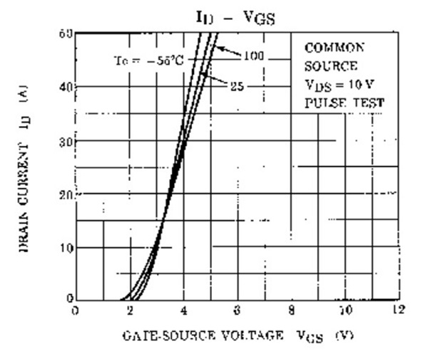
Even if you gradually increase VGS (V), the drain current ID (A) does not flow until it reaches about 2 V.
When VGS exceeds around 2 V, the drain current ID begins to flow.
This boundary voltage is called the threshold voltage (Vth).
Of course, the threshold voltage varies depending on the MOSFET model,
and for the 2SK2232, it can be estimated as roughly 2 V from the curve.
However, there is variation between devices, so keep this in mind.
The threshold voltage is also listed in the datasheet’s electrical characteristics section.
Electrical Characteristics (Ta = 25°C)
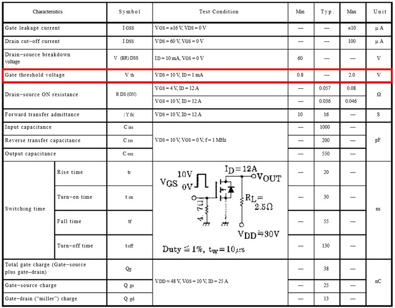
The gate threshold voltage Vth is listed in this section.
At VDS = 10 V and ID = 1 mA, the threshold voltage is specified as Min: 0.8 V and Max: 2.0 V.
This shows that there is significant device-to-device variation.
With such variation, you might wonder:
“What VGS should I apply to ensure the MOSFET definitely turns ON?”
In such cases, one useful approach is to check the switching time section of the datasheet.
The measurement conditions typically show VGS = 10 V being used.
If the device is being switched ON and OFF at 10 V, it means applying 10 V to the gate will certainly turn the MOSFET ON.
*If you are unsure what “turning a MOSFET ON” means, we will explain it clearly later in the “Output Characteristics (VDS–ID Curve)” section.

It is exactly the curve we have discussed so far.
The curve corresponds to the input characteristic graph of the 2SK2232.
The graph can be expressed by the following equation:
ID = K (VGS − Vth)²
This equation describes the relationship between VGS and ID.
(*K is a proportional constant, and it is not listed in the datasheet.)

When ID = 0, the equation becomes VGS = Vth.
Therefore, Vth can be found as the VGS value where ID becomes zero on the input characteristic curve.

The differences are as follows:
Enhancement Type: ID does not flow when VGS = 0.
Depletion Type: ID does flow when VGS = 0.
We will explain this difference from both an “electrical characteristics” and “structural” perspective.
Electrical Characteristics
The Toshiba N-channel MOSFET 2SK2232 is an enhancement-type MOSFET.
If you look at the input characteristic curve, you can see that when VGS = 0, the drain current ID is 0 A.
ID remains at 0 A until VGS reaches around 2 V.
In contrast, let’s look at the input characteristics (VGS–ID curve) of the depletion-type N-channel MOSFET LND150.
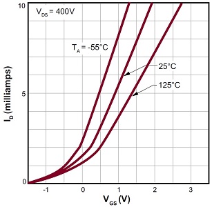
When VGS = 0, the drain current ID flows at about 1–2 A for the depletion-type device.
This shows an important difference in electrical behavior.
The key point is whether current flows or does not flow when VGS = 0.
This difference can be explained by the internal MOSFET structure.
We will look at this structural difference next.
Structure
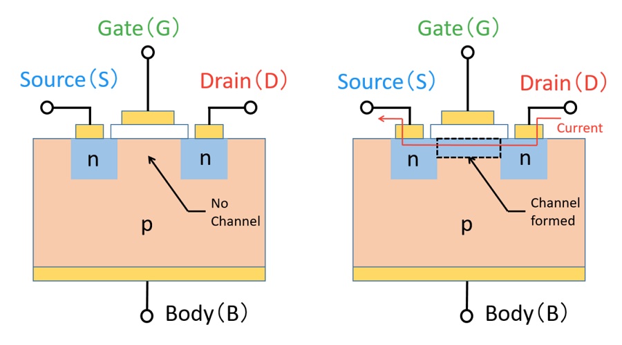
The difference comes from what happens inside the MOSFET when VGS = 0.
Enhancement-type:
The drain current does not flow because the current path (channel) is not formed.
Depletion-type:
The drain current flows because the current path (channel) is already formed.
This is the essential structural difference.
In other words, from a structural perspective, the key distinction is whether the MOSFET has a pre-existing current path when VGS = 0.
When VGS = 0, the question is whether a current channel exists or not.
This explains the fundamental behavioral difference between enhancement and depletion types.
If you want to understand MOSFET structure in more depth, the following article explains it in detail.
Related article: MOSFET Structure and Working Principle Explained
Output Characteristics (VDS – ID Characteristics)
The output characteristics of a MOSFET are shown in the figure below.
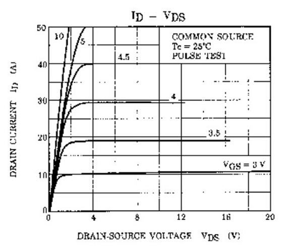
When VGS is fixed at 3 V, increasing VDS gradually causes the drain current ID to rise sharply from 0 A up to about 10 A.
A similar trend appears when VGS is fixed at 3.5 V, 4 V, or 4.5 V. As VDS increases, ID rises quickly from 0 A up to approximately 18 A, 29 A, and 40 A, respectively.
From this graph, two distinct regions can be identified:
① A region where the drain current ID increases rapidly
② A region where the drain current ID becomes nearly constant
These two regions are known as the linear region and the saturation region.
In addition, there is another region where ID remains close to 0 A regardless of the value of VDS.
③ The cutoff region
This region represents the state where the MOSFET is turned off.
These three operating regions correspond to different practical uses of the MOSFET:
① Linear region, ③ Cutoff region → Used for switching ON/OFF
② Saturation region → Used for signal amplification
We will now examine each region in detail.
Linear Region and Cutoff Region
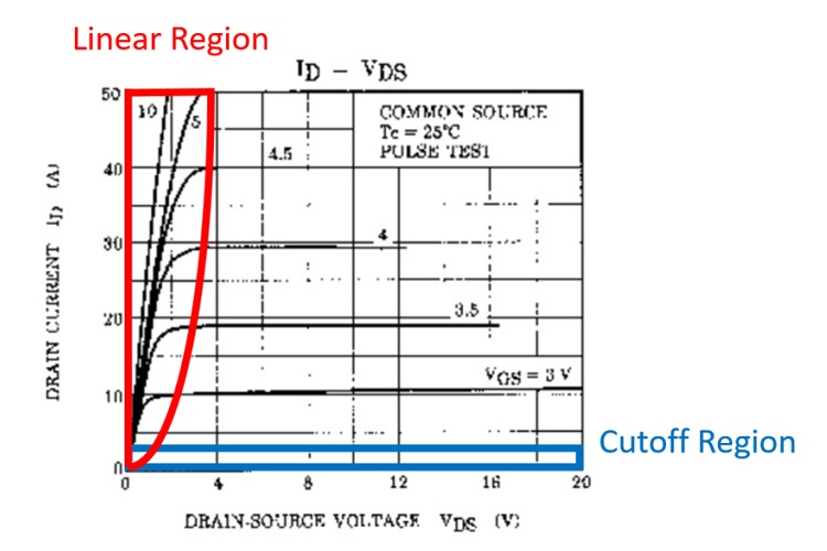
As explained earlier, the region where the drain current ID increases sharply is called the linear region.
It is difficult to define this region by a strict VDS value, but it roughly corresponds to the red-marked area in the figure above.
Similarly, the region where the drain current ID remains close to 0 A is called the cutoff region, shown in the blue-marked area.
These regions allow the MOSFET to be used as a switch.
The reason becomes clear when we consider the characteristics of each region.
Linear region:
VDS is close to 0 V
Cutoff region:
ID is close to 0 A
Let’s compare these characteristics to a typical mechanical switch.
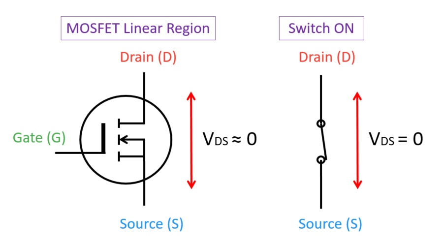
When a switch is ON, the drain–source path is conducting, so VDS becomes nearly 0 V.
Therefore, the MOSFET operating in the linear region corresponds to the switch ON state.
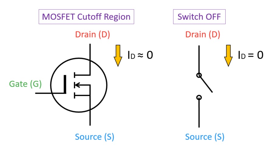
When a switch is OFF, the drain–source path is not conducting, so the drain current ID becomes 0 A.
Thus, the MOSFET operating in the cutoff region corresponds to the switch OFF state.
In summary, when using a MOSFET as a switch:
Linear region → Switch ON
Cutoff region → Switch OFF
These operating principles form the basis of MOSFET switching behavior.
Saturation Region and Pinch-off Voltage
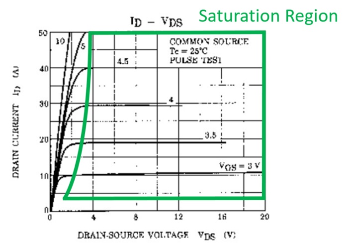
The region where the drain current ID becomes nearly constant is called the saturation region. This corresponds to the green-marked area in the figure.
This region allows the MOSFET to be used for signal amplification.
The reason is that the drain current ID increases in response to the input voltage VGS (gate–source voltage).
For example, from the graph:
At VGS = 3 V, ID = 10 A
At VGS = 3.5 V, ID = 18 A
At VGS = 4 V, ID = 29 A
At VGS = 4.5 V, ID = 40 A
As VGS increases, ID also increases accordingly.
Therefore, when using a MOSFET as an amplifier, this saturation region is utilized.
Also, how does it apply in the static characteristics of a depletion-type MOSFET?
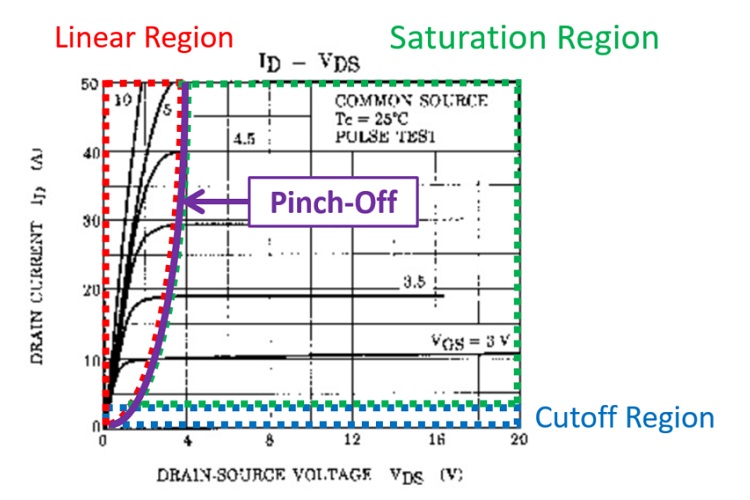
The pinch-off voltage is the boundary between the linear region and the saturation region.
As VDS increases gradually, the operating point transitions from the linear region into the saturation region.
The value of VDS at this transition point is the pinch-off voltage.
The graph shows that the pinch-off voltage increases as VGS increases.
In other words, the pinch-off voltage changes depending on VGS.
As an additional note, when VGS equals the threshold voltage Vth, the pinch-off voltage becomes zero.
Thus, the pinch-off voltage can be expressed as:
Pinch-off Voltage = VGS − Vth
This relationship applies to both enhancement-type and depletion-type MOSFETs.
The same concept can be seen in the characteristics of a depletion-type MOSFET.
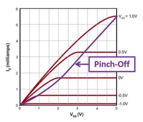
In the LND150 characteristics, the VDS value indicated by the reference line represents the pinch-off voltage.
Generally speaking, a MOSFET with a higher maximum drain current rating is considered to have better performance.
As mentioned earlier, MOSFETs can be used as switches.
If you compare a “switch that can handle 1 A” with one that can handle 5 A,
the switch that can handle 5 A is generally considered superior.
However, this does not always apply when operating at high frequencies.
The reason is that MOSFETs with higher current ratings typically have larger gate capacitance,
which can make high-frequency ON/OFF switching more difficult.
How to Measure MOSFET Static Characteristics (Input and Output Characteristics)
Measuring the input and output characteristics of a MOSFET is not difficult.
The basic measurement circuit is shown below.
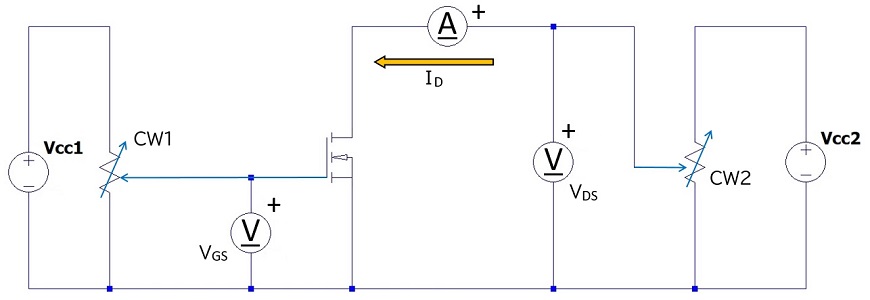
Measurement circuit for MOSFET static characteristics
VGS is adjusted using the input variable resistor (CW1).
VDS is adjusted using the output variable resistor (CW2).
To measure the input characteristic (VGS–ID),
fix VDS at a constant voltage and gradually increase VGS.
Measure the drain current ID and plot it on a graph to obtain the input characteristic.
To measure the output characteristic (VDS–ID),
fix VGS at a constant voltage and gradually increase VDS.
Measure the drain current ID and plot it on a graph to obtain the output characteristic.
However, there is one important point to note.
When measuring a power MOSFET that handles large currents, the device may heat up, making accurate measurement impossible.
Therefore, manufacturers use pulsed measurement to reduce heat during testing.
For example, the Toshiba 2SK2232 is also a power MOSFET.
In this case, the datasheet contains descriptions such as “PULSE TEST”
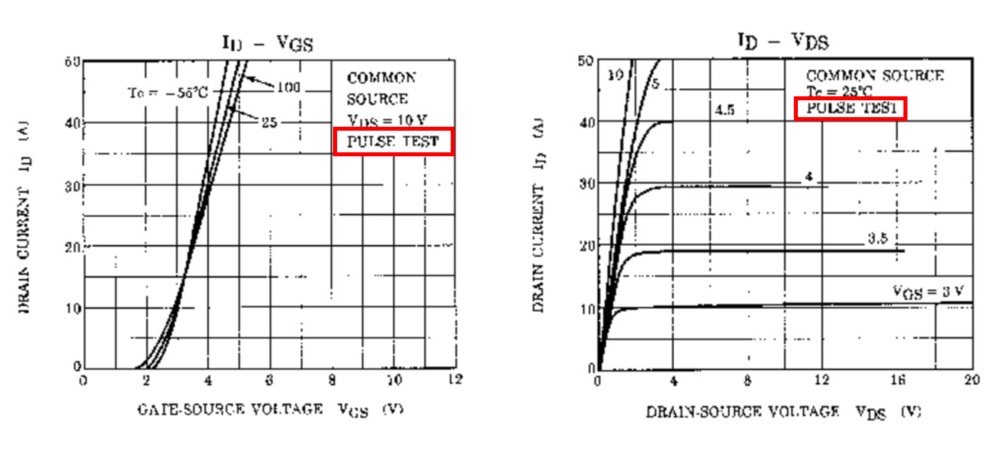
When pulse measurement is required, follow the measurement conditions listed in the datasheet.
However, some datasheets do not provide the measurement conditions.
In that case, the only option is to contact the manufacturer.
As explained so far, these measurements reveal the intrinsic characteristics of the MOSFET.
If the datasheet provides this information, you do not need to measure it yourself.
However, some MOSFET datasheets do not include static characteristics.
In such cases, measurement becomes necessary.
Personally, I do not recommend choosing MOSFETs whose datasheets lack static characteristic information.
If the device is reliable, the manufacturer would normally provide these characteristics.
In any case, static characteristics are essential because they determine how the MOSFET should be used in a circuit.
They are arguably the most important parameters of the MOSFET.
So it is important to understand them thoroughly.
Let’s Actually Measure the MOSFET Characteristics!
Let’s build a simple circuit and measure the MOSFET’s input and output characteristics in practice.
Required Components
- MOSFET 2N7000
-
An enhancement-type N-channel MOSFET ideal for static characteristic experiments.
- Potentiometer Set (Variable Resistors)
-
Used to vary the gate voltage and observe changes in the drain current.
- Breadboard (830 holes)
-
A solderless breadboard makes it easy to modify circuits during testing.
- Jumper Wire Set
-
Wires used to connect components on the breadboard.
- USB 5 V Breadboard Power Module
-
Provides 5 V or 3.3 V directly to the breadboard. Very convenient for quick experiments.
- Digital Multimeter (Tester)
-
Used to measure gate voltage VGS and drain current ID when plotting characteristic curves.
Important Notes
MOSFET pin configurations may vary depending on the manufacturer and model.
Also, the maximum voltage and current ratings differ by product.
Always check the datasheet for pin layout and ratings before building your circuit.
Useful Tools for Measurement
If you want to check “What is the threshold voltage?” or “In which region is the current changing?”, measurement tools will help.
Try using the following instruments:
- To easily check voltage and current: → Digital Multimeter
- To observe signal waveforms: → Oscilloscope
- To power your circuit safely with a stable source: → DC Power Supply
Summary
In this article, we explored the static characteristics of MOSFETs.
Were you able to understand how the input and output characteristics behave?
I hope this guide helps you when analyzing MOSFET behavior in your own circuits.